Easyeda eda pcb powerful Relay circuit easyeda using schematic mcu switch buzzer driver pcb programmable capture pic tool drawn example simulation layout cloud based Easyeda pcb design: a comprehensive guide – hillman curtis: printed
How to Use EasyEDA to design PCB Schematic Step By Step
How to prototype a pcb schematic with easy eda How to use easyeda to design pcb schematic step by step Getting started with easyeda part 3: pcb layout – shawn hymel
Easyeda : circuit design, simulation, pcb layout, pcb ordering & uses
Circuit board easyeda copper traces hereEasyeda : features, circuit design and simulation Easyeda pcb circuitsHow to use easyeda to design pcb schematic step by step.
Easyeda circuit design: a beginner’s guide to creating professional pcbEasyeda pcb schematic Pcb easyeda using simple circuit project designing tool tutorial complete logging after clickEasyeda circuit pcb watelectronics.

Easyeda pcb software schematic project board electronics convert layout started getting part outline lab button click components
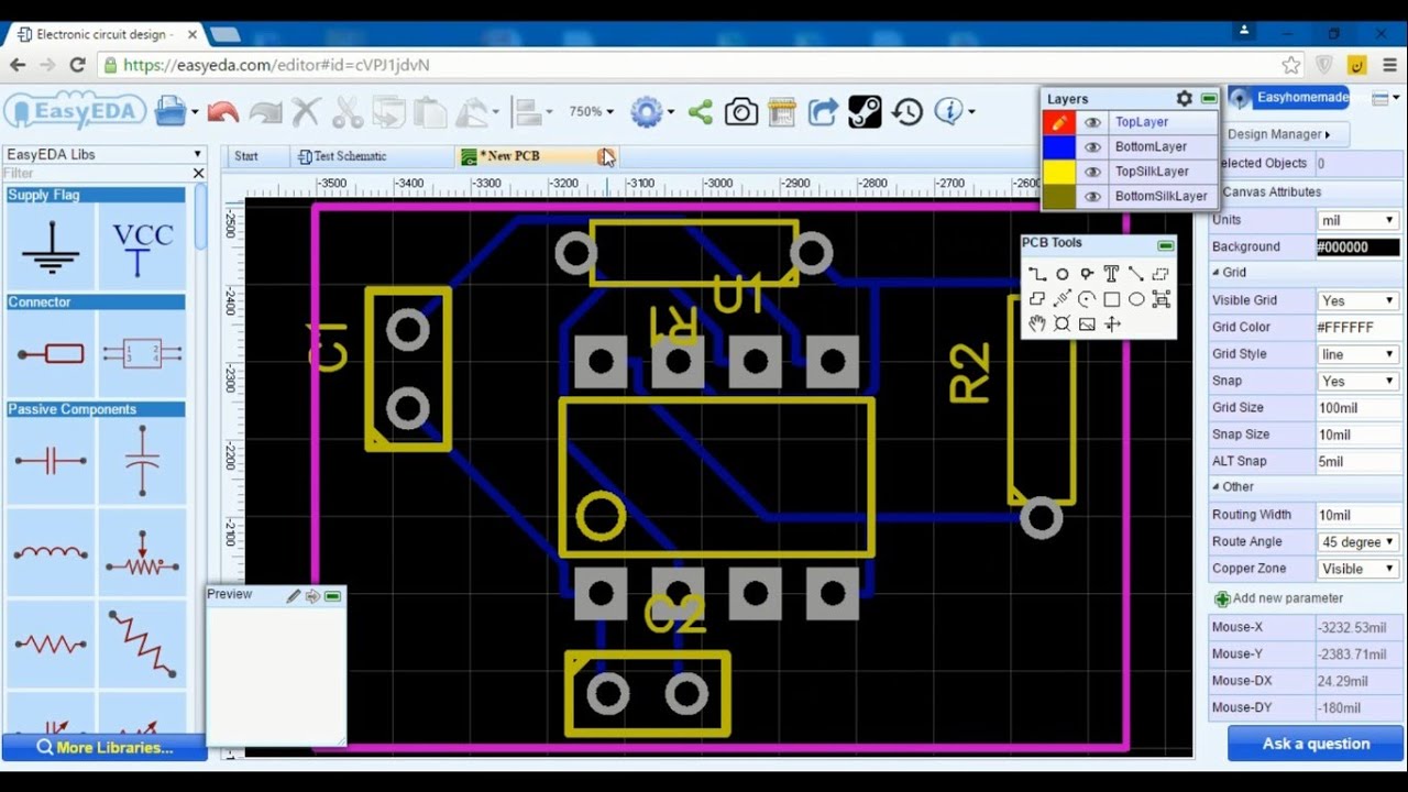
Easyeda schematic diagramUsing easyeda to design and build a pcb (printed circuit board) Getting started with easyeda part 3: pcb layout – shawn hymelEasyeda pcb layout started getting part.
Easyeda: getting started with pcb design!Arduino nano board circuit diagram How to use easyeda pcb circuit simulator – hillman curtis: printedEasyeda pcb layout started getting part schematic exporting.

How to design a pcb easily with easyeda
Easyeda: a free cloud-based tool for schematic capture, pcb layout, andComplete pcb designing tutorial using easyeda pcb design tool Easyeda pcbGetting started with easyeda part 3: pcb layout – shawn hymel.
Pcb easyedaDownload & tutorial of easyeda online pcb software Descargar gratis easyeda: simulación de circuitos, diseño de circuitoCreate circuit schematics and pcb using easyeda and proteus by.

Easyeda circuit board design
Simulation easyeda circuit pcbEasyeda pcb Easyeda-easy to design pcb. what is a printed circuit board(pcb)? aEasyeda tutorial.
Easyeda : circuit design, simulation, pcb layout, pcb ordering & usesFree online schematic creator How to use easyeda pcb circuit simulator – hillman curtis: printed(a) the pcb of the new board in 2d using easyeda, (b) the pcb of the.
Easyeda pcb layout started getting part outline board delete ahead purple go
Easyeda circuit pcb schematic cloud software basedEasyeda: a free cloud-based tool for schematic capture, pcb layout, and Easyeda schematicEasyeda kicad eagle embedded lab lib thousands gives access source open pcb capture schematic circuit simulation tool based layout cloud.
Pcb easyeda jlcpcbGetting started with easyeda part 3: pcb layout – shawn hymel How to design a pcb easily with easyeda & jlcpcbEasyeda eda prototyping ports schematics difficult visually.


EasyEDA circuit board design

How to Use EasyEDA to design PCB Schematic Step By Step

EasyEDA: A free cloud-based tool for schematic capture, PCB layout, and

EasyEDA : Features, Circuit Design and Simulation

EasyEDA : Circuit Design, Simulation, PCB Layout, PCB Ordering & Uses

EasyEDA : Circuit Design, Simulation, PCB Layout, PCB Ordering & Uses

How to Prototype a PCB Schematic with Easy EDA
